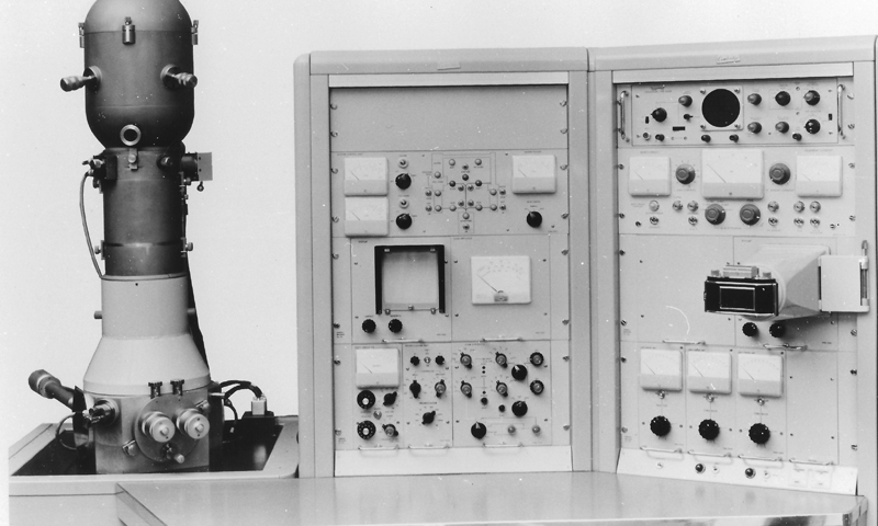
The Scanning Electron Microscope
Professor Sir Charles William Oatley (1904-96) from Somerset worked on developing the scanning electron microscope (SEM) for two decades. During WW2 he was involved in radio and radar technology and then furthered his inventive talent with his PhD students in his laboratory at the University of Cambridge, where he himself had been educated. He felt they would learn more by dealing with a real breakthrough challenge.
Eleven fledgling engineers ~ Messrs. Sander, McMullan, Smith, Wells, Everhart, Thornley, Spreadbury, Stewart, Broers, Ahmed and Pease ~ successively assisted Oatley in making gradual, significant improvements to his SEM prototype, until it was finally presented to the scientific market in 1965. Oatley had picked up the initial idea from groundwork in Germany and the USA that had been abandoned.
Whole objects can be placed under the microscope’s electron beam, as opposed to the ultra-thin slices required for its predecessor, the transmission electron microscope. Another benefit is the three-dimensional magnification that it produces on the computer screen, thanks to the configuration of lenses, coils, etc., and the addition of a raster scanner that zigzags over the specimen. There are numerous applications for the SEM, wherever materials analysis or investigation are needed and over 50,000 SEM instruments have been sold worldwide.
(Image of one of the early Cambridge SEMs: Zeiss Microscopy at Wikimedia Commons / CC BY-SA 2.0)
